![]()
Today the first Photonic Integrated Circuit Conference came to a close , which took place simultaneously with the 6th edition of the compound semiconductor industry conference in a rainy Brussels. PhotonTransfer would like to present some important take-aways from the event.
The exponential increase in web traffic and cloud applications is leading to the development of mega Datacenters which are demanding higher bandwidth, less cooling needs and more power efficiency. It is and excellent opportunity to fully bring optics inside data centers. In order to do this Integration is an important factor. However, standardization and hyper-scale production of Photonic Integrated Circuits like in the semiconductor industry is a requirement for companies such as Microsoft. The research and the industry as a whole are almost there, but the following issues need to be addressed:
- The packaging of the Photonic Integrated Circuit (PIC) is one of the bottle necks for mass production. Today it represents 70% to 80% of the cost of a PIC.
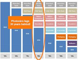
- The complete outsourcing process of the integrated device manufacturer (IDM) industry was one of the key elements that contributed to electronic mass production, and VLC Photonics (one of the main PIC design houses) benchmarked the PIC industry´s current outsourcing situation in regards to the semiconductor industry, resulting in 30 years of delay.
- The Laser which is the source for several modules hasn’t being clearly integrated, which was an issue that was point out in the first conference block.
The tools for designing, making packaging and testing Photonic Integrated Circuits are almost there:
At the design level, not all the semiconductor tools can be exported to the PIC sector. The EDA (electronic design automation) from the semiconductor industry still doesn´t have its EPDA efficient equivalent.
There are still no standards for Photonic Integrated Circuits and we can see it at the material level:
Three main material platforms are available today for the Multi Project Wafer (MPW) in different foundries: Indium Phosphide (InP) – TriPleX (Si3N4) – Silicon Photonics (SOI).
There is still no Intellectual Property business model for designing PIC unlike in the semiconductor industry. Several foundries are applying an open innovation and technology transfer model by opening their platform for all users like the well-known IMEC foundry in Belgium. The recently created American Institute for Manufacturing Integrated Photonics (AIM Photonics) is largely inspired by this European Open Innovation model as his director told PhotonTransfer in San Francisco Photonics West Exhibtion.
EPDA, packaging, IP business, laser integration and standardization are not quite there yet. However the need is prevalent as high traffic growth, giant cloud datacenters and also for more value added application for example biosensors for POC (Point of care devices) requiring low cost chip in the health sector.