“Graphene is going to change the world—or so we’ve been told”– Phys.org
What is graphene?
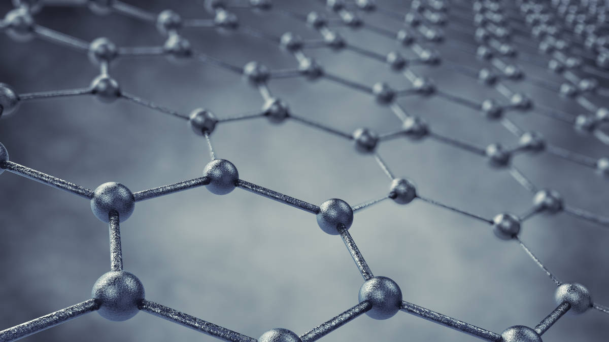
Graphene is a brand new material first isolated by scientists in 2004 formed by a single-atom thick layer of carbon atoms arranged in a hexagonal lattice. It has high electron mobility and it is thought to be the new high-tech material of the 21st century.
How is it made?
There are at least four methods of production:
- Metal exfoliation
- Using an atomic microscope; these first two methods involve stripping down graphite into thinner and thinner pieces, resulting in a substance which is one atom thick. This is a very long and laborious task and the reason why this is one of the most expensive materials in the world.
- Chemical vapor deposition; here a carbon based gas is put into a container with a conductive metal. By manipulating the pressure and temperature inside the container, layers of graphene begin to form. This method could allow the mass production, which may be a solution to its current high cost of production.
- Growing graphene crystals; Scientists start with a high carbon substance such as sugar and manipulate it in a way that enables them to grow graphene crystals out of it. This method is still in its “experimental stage” but could also be a viable solution to the high cost of production.
Properties
Graphene is a single layer of graphite laid out on a honeycomb lattice, which has unusual optical and electronic properties. Graphene is approximately 200x stronger than steel but a lot thinner and is practically impermeable to gases. It conducts less heat as the temperature increases, which allows it to withstand high heat. Graphene is also made of carbon, which is the fourth-most abundant element in Earth’s atmosphere. What makes graphene useful is its ability to bend, stretch and roll while still maintaining its other properties.
The applications
There are several important potential uses of graphene, these include:
- Detecting and Converting light into electrical signals, which is at the heart of many technologies we use today. For example, video imaging, optical communications, biomedical imaging, security, night vision, gas sensing, wearable health devices and motion detection. The demand for faster sensors and imaging systems is increasing and existing technologies are limited. One example of a technology is the High Bandwidth Photodetector.
- Benefits of 2D materials graphene is gapless and therefore absorbs light in the UV, visible, short-wave infrared, near-IR, mid-IR, far-IR and THz spectrums. 2D materials can also be integrated with silicon electronics which means that graphene can be used in electronical items for high resolution imaging or spectroscopy systems.
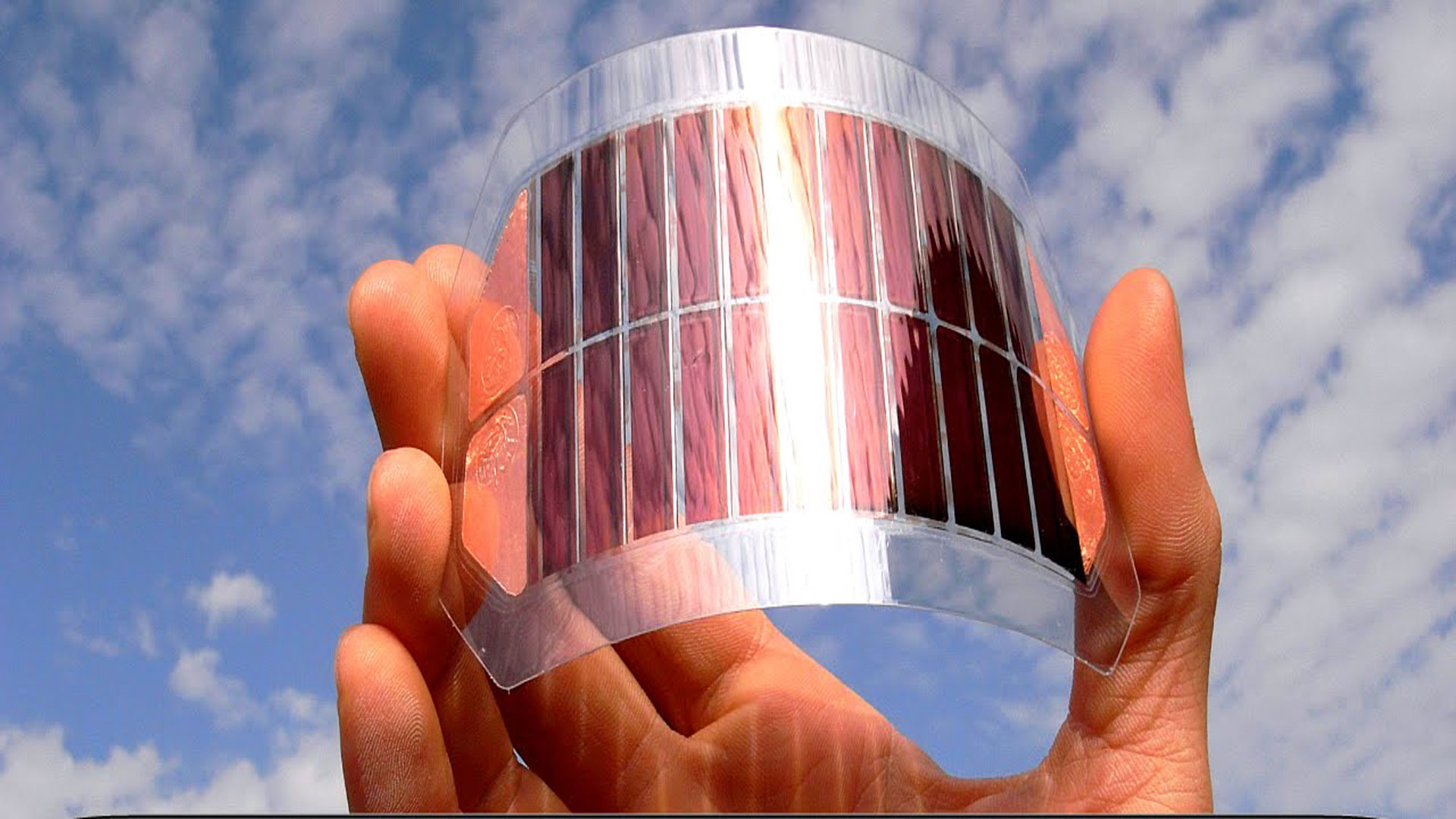
- Longer battery life Graphene anodes result in faster battery charging and discharging compared to conventional anodes. Graphene batteries are in the experimentation stage but universities worldwide such as Rice University in Texas, USA are experimenting with the addition of boron in batteries to help the lithium ions stick to the graphene anodes.
- Internet of Things- due to its unique properties, and the emergence of ´flexible electronics´, wearable electronics and the Internet of things, there is a lot of potential for graphene. Many of this new technology requires components which are flexible and foldable. If made affordable, this technology could be a competitive alternative to for applications in health, security and automotive systems.
The advantages
- Strength- It´s approximately 200x stronger than steel
- Conductivity- it´s one of the most conductive metals on earth
- Hardness- It’s harder than diamond
- Flexibility- Only one atom thick, which allows it to bend and move easily
- Silicon integration- graphene photo detector arrays can be monolithically integrated with multi-megapixel read-out electronics.
The disadvantages
- Expensive- The first methods mentioned in this article are very time-consuming resulting in the material being very expensive to produce; this will be the case until scientists figure out an efficient way for mass production.
- Lack of band gap- this means the minimum amount of energy for an electron to break free. The lack of band gap causes electrons to flow freely, and therefore causing graphene to act more like a metal than a semi-conductor. This can cause issues as it prevents the ability to switch its properties on or off.
- Lack of purity- graphene has the potential to be useful for things such as quantum computing and electronics, but it needs to be “perfect” in order for it to be effective.
The future
According to an article in Inquisitr “If you have a material that’s one atom thick, it’s going to be really affected by its environment. If the graphene is on top of something that’s rough and disordered, it’s going to interfere with how the electrons move. It’s really important to create graphene with no interference from its environment.”
Currently, scientists are trying to figure out the most effective way to transfer heat energy using graphene. It is necessary that graphene is better understood, can be made “perfect” for its uses and be mass produced in a way which is cost effective. Once this happens it has the ability to change the world around us.
Conclusions
To conclude, graphene is a material with extremely unique and useful properties. It´s strength, hardness, electrical and heat conductivity, flexibility and silicon integration means it has the potential to be useful in a variety of electronic and high tech products. It could be used in computer science, touch screen electronics, in the ´Internet of Things´ devices such as health wearable’s and for optical communications.
However due to the method of production, it is currently very expensive to make and not particularly pure. With more scientific research and effective methods of mass production, it can be used effectively in our everyday lives and change the way in which we live.
PhotonTransfer is the world’s first open innovation marketplace specializing in photonics. We have a range of tech for transfer listings which involve new technology looking for collaboration to help get it to market. Look for specific technologies available for transfer among our listings here.
In the mean time feel free to check out our website http://photontransfer.com/ for more information about how we bridge the gap between science and market.